
Services
Browse all products ›
 Mining & Oil & Gas Services
7 active subcategories
Building & Construction & Maintenance Services
2 active subcategories
Industrial Production & Manufacturing Services
9 active subcategories
Industrial Cleaning Services
4 active subcategories
Environmental Services
4 active subcategories
Transportation & Storage & Mail Services
6 active subcategories
Management & Business Professionals & Administrative Services
7 active subcategories
Engineering & Research & Technology Based Services
7 active subcategories
Editorial & Design & Graphic & Fine Art Services
6 active subcategories
Public Utilities & Public Sector Related Services
3 active subcategories
Financial & Insurance Services
5 active subcategories
Healthcare Services
7 active subcategories
Education & Training Services
5 active subcategories
Travel & Food & Lodging & Entertainment Services
6 active subcategories
Personal & Domestic Services
2 active subcategories
National Defense & Public Order & Security & Safety Services
1 active subcategories
Politics & Civic Affairs Services
4 active subcategories
Organizations & Clubs
3 active subcategories
Mining & Oil & Gas Services
7 active subcategories
Building & Construction & Maintenance Services
2 active subcategories
Industrial Production & Manufacturing Services
9 active subcategories
Industrial Cleaning Services
4 active subcategories
Environmental Services
4 active subcategories
Transportation & Storage & Mail Services
6 active subcategories
Management & Business Professionals & Administrative Services
7 active subcategories
Engineering & Research & Technology Based Services
7 active subcategories
Editorial & Design & Graphic & Fine Art Services
6 active subcategories
Public Utilities & Public Sector Related Services
3 active subcategories
Financial & Insurance Services
5 active subcategories
Healthcare Services
7 active subcategories
Education & Training Services
5 active subcategories
Travel & Food & Lodging & Entertainment Services
6 active subcategories
Personal & Domestic Services
2 active subcategories
National Defense & Public Order & Security & Safety Services
1 active subcategories
Politics & Civic Affairs Services
4 active subcategories
Organizations & Clubs
3 active subcategories
Gifts, Sports & Toys
Browse all products ›

Machinery, Industrial Parts & Tools
Browse all products ›
 Mining & Well Drilling Machinery & Accessories
5 active subcategories
Farming & Fishing & Forestry & Wildlife Machinery & Accessories
2 active subcategories
Building & Construction Machinery & Accessories
1 active subcategories
Industrial Manufacturing & Processing Machinery & Accessories
19 active subcategories
Material Handling & Conditioning & Storage Machinery & their Accessories & Supplies
5 active subcategories
Power Generation & Distribution Machinery & Accessories
5 active subcategories
Tools & General Machinery
4 active subcategories
Structures & Building & Construction & Manufacturing Components & Supplies
14 active subcategories
Manufacturing Components & Supplies
29 active subcategories
Distribution & Conditioning Systems & Equipment & Components
4 active subcategories
Laboratory & Measuring & Observing & Testing Equipment
3 active subcategories
Cleaning Equipment & Supplies
4 active subcategories
Service Industry Machinery & Equipment & Supplies
2 active subcategories
Mining & Well Drilling Machinery & Accessories
5 active subcategories
Farming & Fishing & Forestry & Wildlife Machinery & Accessories
2 active subcategories
Building & Construction Machinery & Accessories
1 active subcategories
Industrial Manufacturing & Processing Machinery & Accessories
19 active subcategories
Material Handling & Conditioning & Storage Machinery & their Accessories & Supplies
5 active subcategories
Power Generation & Distribution Machinery & Accessories
5 active subcategories
Tools & General Machinery
4 active subcategories
Structures & Building & Construction & Manufacturing Components & Supplies
14 active subcategories
Manufacturing Components & Supplies
29 active subcategories
Distribution & Conditioning Systems & Equipment & Components
4 active subcategories
Laboratory & Measuring & Observing & Testing Equipment
3 active subcategories
Cleaning Equipment & Supplies
4 active subcategories
Service Industry Machinery & Equipment & Supplies
2 active subcategories
Transportation
Browse all products ›

Mineral, Textile, Herbal and Animal Products
Browse all products ›

Agriculture & Food
Browse all products ›

Health & Beauty
Browse all products ›

Oil, Gas, Chemical, Rubber and Plastics
Browse all products ›

Electric, Electronics and Telecommunications
Browse all products ›
 Electronic Components & Supplies
6 active subcategories
Electrical systems & Lighting & components & accessories & supplies
4 active subcategories
Information Technology Broadcasting & Telecommunications
5 active subcategories
Defense & Law Enforcement & Security & Safety Equipment & Supplies
5 active subcategories
Electronic Components & Supplies
6 active subcategories
Electrical systems & Lighting & components & accessories & supplies
4 active subcategories
Information Technology Broadcasting & Telecommunications
5 active subcategories
Defense & Law Enforcement & Security & Safety Equipment & Supplies
5 active subcategories
Apparel,Textiles & Accessories
Browse all products ›

Packaging, Advertising & Office
Browse all products ›


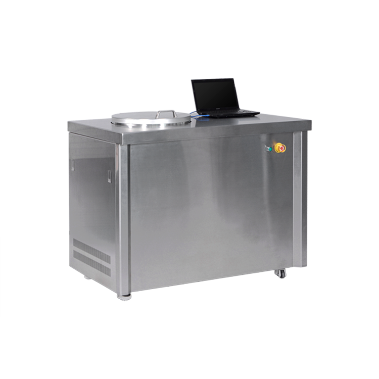
Multi-Piece Plasma Enhanced Atomic Layer Deposition System for The Deposition of Thin Films of Temperature-Sensitive Materials

The PEALD-B plasma-enhanced atomic layer deposition system is a multi-chip deposition system specially designed for scientific research and industrial development users in special application fields. The electrical system of the system is fully compliant with CE standards; this system extends the co...
The PEALD-B plasma-enhanced atomic layer deposition system is a multi-chip deposition system specially designed for scientific research and industrial development users in special application fields. The electrical system of the system is fully compliant with CE standards; this system extends the common atomic layer deposition system to precursors The selection range of the source, increase the film deposition rate and reduce the deposition temperature, are widely used in the deposition of temperature-sensitive materials and films on flexible substrates.
Product advantages:
Advanced software control system: The system integrates functions such as process recipe, parameter setting, authority setting, interlocking alarm, and status monitoring;
Technical index:
The size of the substrate is 8 inches and below
The substrate heating temperature: room temperature~500℃, control accuracy ±0.1℃
Precursor transport system Standard 3-way precursor pipeline, optional
Precursor pipeline temperature: room temperature~200℃, control accuracy ±0.1℃
Heating temperature of source bottle: room temperature~200℃, control accuracy ±0.1℃
ALD valve Swagelok fast high temperature ALD special valve
Background vacuum <5*10-5Torr, imported anticorrosive pump
Carrier gas system N2 or Ar
Processing capacity 500 pieces of 8 inches
Growth mode High-speed deposition mode and dwell growth mode
Plasma source 300W inductively coupled remote plasma
Plasma discharge gas source Standard 3 channels, optional
Control system PLC+touch screen or display
Power supply 50-60Hz, 220V/20A AC power supply
Non-uniformity of deposition Non-uniformity<±1%
Equipment size 1300mm x 800mm x 1000mm
Types of deposited films:
Elementary substance: Co, Cu, Ta, Ti, W, Ge, Pt, Ru, Ni, Fe...
Nitride: TiN, SiN, AlN, TaN, ZrN, HfN, WN…
Oxide: TiO2, HfO2, SiO2, ZnO, ZrO2, Al2O3, La2O3, SnO2...
Other compounds: GaAs, AlP, InP, GaP, InAs, LaHfxOy, SrTiO3, SrTaO6...
ALD application examples:
High-K gate oxide layer, storage capacitive dielectric, high aspect ratio diffusion barrier in copper interconnection, pinhole-free passivation layer for OLED, high uniform coating of MEMS, nanoporous structure coating, special fiber doping, solar cell, flat panel Displays, optical films, and other types of nano films with special structures
| Attribute name | Attribute value |
|---|---|
| Product Features | |
| Color | Silver, Golden gray |
| Measurement method | Vacuum gauge, Temperature controller |
| Performance | automatic, multi-function, wide application, High precision |
| Standards | According to customer requirements, CE |
| Warranty | 1Year |
| After Sale Services | lifetime |


")