
Services Browse all products ›
 Mining & Oil & Gas Services 7 active subcategories Building & Construction & Maintenance Services 2 active subcategories Industrial Production & Manufacturing Services 9 active subcategories Industrial Cleaning Services 4 active subcategories Environmental Services 4 active subcategories Transportation & Storage & Mail Services 6 active subcategories Management & Business Professionals & Administrative Services 7 active subcategories Engineering & Research & Technology Based Services 7 active subcategories Editorial & Design & Graphic & Fine Art Services 6 active subcategories Public Utilities & Public Sector Related Services 3 active subcategories Financial & Insurance Services 5 active subcategories Healthcare Services 7 active subcategories Education & Training Services 5 active subcategories Travel & Food & Lodging & Entertainment Services 6 active subcategories Personal & Domestic Services 2 active subcategories National Defense & Public Order & Security & Safety Services 1 active subcategories Politics & Civic Affairs Services 4 active subcategories Organizations & Clubs 3 active subcategories
 Gifts, Sports & Toys Browse all products ›

Machinery, Industrial Parts & Tools Browse all products ›
 Mining & Well Drilling Machinery & Accessories 5 active subcategories Farming & Fishing & Forestry & Wildlife Machinery & Accessories 2 active subcategories Building & Construction Machinery & Accessories 1 active subcategories Industrial Manufacturing & Processing Machinery & Accessories 19 active subcategories Material Handling & Conditioning & Storage Machinery & their Accessories & Supplies 5 active subcategories Power Generation & Distribution Machinery & Accessories 5 active subcategories Tools & General Machinery 4 active subcategories Structures & Building & Construction & Manufacturing Components & Supplies 14 active subcategories Manufacturing Components & Supplies 29 active subcategories Distribution & Conditioning Systems & Equipment & Components 4 active subcategories Laboratory & Measuring & Observing & Testing Equipment 3 active subcategories Cleaning Equipment & Supplies 4 active subcategories Service Industry Machinery & Equipment & Supplies 2 active subcategories
 Transportation Browse all products ›

Mineral, Textile, Herbal and Animal Products Browse all products ›

Agriculture & Food Browse all products ›

Health & Beauty Browse all products ›

Oil, Gas, Chemical, Rubber and Plastics Browse all products ›

Electric, Electronics and Telecommunications Browse all products ›
 Electronic Components & Supplies 6 active subcategories Electrical systems & Lighting & components & accessories & supplies 4 active subcategories Information Technology Broadcasting & Telecommunications 5 active subcategories Defense & Law Enforcement & Security & Safety Equipment & Supplies 5 active subcategories
 Apparel,Textiles & Accessories Browse all products ›

Packaging, Advertising & Office Browse all products ›


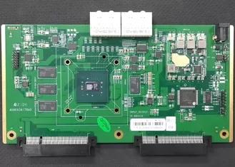
Thru Hole SMT OSP FR4 Electronics Automotive PCB Assembly

PCB Assembly Introduction For Turnkey PCB Assembly, all you need to do is to send us your PCB assembly Bill of Materials (BOM) list. ( a document or a spreadsheet format containing the PCB specification selection ), the number of layers, quantity, and all dimensions necessary. In addition, you al...
PCB Assembly Introduction
For Turnkey PCB Assembly, all you need to do is to send us your PCB assembly Bill of Materials (BOM) list. ( a document or a spreadsheet format containing the PCB specification selection ), the number of layers, quantity, and all dimensions necessary. In addition, you also need to include a CAD-generated Gerber or Centroid file for the top/bottom copper, Silkscreen and other details.
Next, we will send a formal quote for your order approval before production . you can fix it if there’s any problem .
A summary of the process for a turnkey PCB assembly order :
Place Order
Component procurement
PCB Design
PCB Assembly
Quality assurance and testing
Prototyping
Packing
Shipping
Aftersales services and support
PCB CAPABILITIES
FACTORY CAPABILITIES
No. Items 2019 2020
1 HDI Capabilities HDI ELIC (4+2+4) HDI ELIC(5+2+5)
2 Max layer count 32L 36L
3 Board Thickness Core thickness 0.05mm-1.5mm ,Fineshed board thickness 0.3-3.5mm Core thickness 0.05mm-1.5mm ,Fineshed board thickness 0.3-3.5mm
4 Min.Hole Size
Laser 0.075mm
Mechnical 0.15
Laser 0.05mm
Mechnical 0.15
5 Min Line Width/Space 0.035mm/0.035 0.030mm/0.030mm
6 Copper Thickness 1/3oz-4oz 1/3oz-6oz
7 Size Max Panel size 700x610mm 700x610mm
8 Registration Accuracy +/-0.05mm +/-0.05mm
9 Routing Accuracy +/-0.075mm +/-0.05mm
10 Min.BGA PAD 0.15mm 0.125mm
11 Max Aspect Ratio 10:1 10:1
12 Bow and Twist 0.50% 0.50%
13 Impedance Control Tolerance +/-8% +/-5%
14 Daily output 3,000m2 (Max capacity of equipment) 4,000m2 (Max capacity of equipment)
15 Surface Finishing HASL Lead Free /ENEPING /ENIG /HASL /FINGER GOLD/IMMERSION TIN/SELECTIVE THICK GOLD
16 Raw Material FR-4/Normal Tg/High Tg/Low Dk/HF FR4/PTEE/PI


